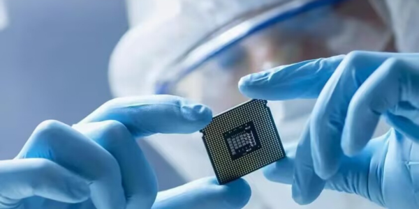
Improving wafer fabrication processes and exploring full-spectrum plasma monitoring solutions for etch endpoints
Views : 14
Update time : 2022-10-21 12:02:42
Meeting the demands of today's booming technology innovation and complex and changing industrial environment, semiconductor foundries require quantitative, accurate and high-speed process measurements. Ocean Insight has partnered with a leading innovator in plasma etch technology to explore full-spectrum plasma monitoring solutions for detecting critical wafer etch endpoints.
The challenge for customers
With the global demand for semiconductors growing rapidly, the industry is well positioned to invest in cost-saving process improvements and the development of increasingly complex semiconductor designs and formulations. To meet today's technology boom and respond to the expanding market, semiconductor foundries need quantitative, accurate and high-speed process measurements.
Semiconductors and microelectromechanical systems (MEMS) are reaching their design limits and further improvements by reducing size or increasing speed are almost impossible. Instead, manufacturers are focusing on wafer quality, repeatability and overall yield, as well as increasing throughput. The goal is to meet the growing demand for smart electronics while keeping production costs and prices competitive.
Our view
Rapid analysis of weak plasma or wafer spectra can help refine etch process parameters while improving wafer quality. Spectrometer-based plasma measurements combined with powerful software can account for the changing state of plasma, chamber and viewport conditions and are sensitive to the weakest signals from deep etch or thin design features.
Spectroscopy helps to make end-point detection more accurate, allowing more complex wafer shapes and patterns to be designed. Smaller features can be manufactured as manufacturers can stop and start the production process more accurately, while reducing errors and decreasing the amount of unavailable space on the wafer. In addition, as endpoint detection becomes more accurate, thinner layers of different materials can be used, even if they produce weak, indistinguishable spectral features and more closely spaced peaks.
The solution
Ocean Optics has partnered with leading equipment suppliers to the semiconductor industry to advance endpoint inspection technology. We have customised our spectrometers (the Ocean SR2 and Ocean HDX are ideal for plasma monitoring applications) to provide the fast, high sensitivity, precise resolution and versatile connectivity required for semiconductor manufacturing.
With Ocean Optics hardware and support, the equipment supplier continues to improve and refine its etch technology for the semiconductor industry. Its leadership in plasma processing and advanced packaging solutions supports emerging technologies associated with wireless devices, photonics, solid state lighting and MEMS devices.

 How many chips does a car need?
 Position and Function of Main Automotive Sensors
 Chip: The increasingly intelligent electronic brain
 LDA100 Optocoupler: Outstanding Performance, Wide Applications
