 Resistance Thermometer Temperature Sensors
Dec .31.2024
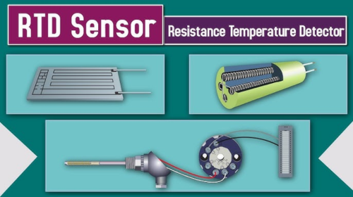
A resistance thermometer is a common temperature sensor that measures temperature by utilizing the property that the resistance of materials changes with temperature. Resistance thermometers are widely used in various fields, including industrial control,
 Say Goodbye to Lag! Three Ways to Speed Up WiFi
Dec .31.2024
Don't worry. By learning the following three methods, your WiFi experience can be greatly improved! Let's improve the home WiFi signal from three aspects: transmission power, wireless channels, and location with the agency of Cirrus Logic. Say goodbye to


 How to Identify Legitimate Sellers When Purchasing Electronic Components Online?
 Development Directions and Innovation Trends of the Electronic Components Market in 2025
 Resistance Thermometer Temperature Sensors
 Say Goodbye to Lag! Three Ways to Speed Up WiFi
