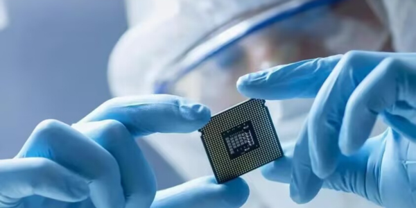
 How many chips does a car need?
Sep .19.2024
Automotive chips can be divided into four types according to their functions: control (MCU and AI chips), power, sensors, and others (such as memory). The market is monopolized by international giants. The automotive chips people often talk about refer to
 Position and Function of Main Automotive Sensors
Sep .18.2024
The function of the air flow sensor is to convert the amount of air inhaled into the engine into an electrical signal and provide it to the electronic control unit (ECU). It is the main basis for determining the basic fuel injection volume. Vane type: The
 Chip: The increasingly intelligent electronic brain
Sep .14.2024
In this era of rapid technological development, we often marvel at how mobile phones can run various application software smoothly, how online classes can be free of lag and achieve zero latency, and how the functions of electronic devices are becoming mo
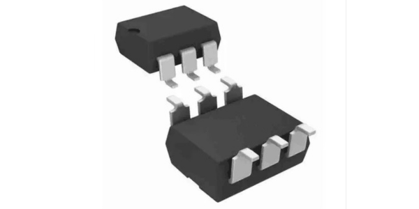 LDA100 Optocoupler: Outstanding Performance, Wide Applications
Sep .13.2024
In terms of characteristics, LDA100 is outstanding. It offers AC and DC input versions for optional selection, enabling it to work stably in different power supply environments. The small 6-pin DIP package not only saves space but also facilitates install


 How many chips does a car need?
 Position and Function of Main Automotive Sensors
 Chip: The increasingly intelligent electronic brain
 LDA100 Optocoupler: Outstanding Performance, Wide Applications
